1 the introduction
In the LED industry chain, the upstream is LED substrate chip and substrate production, the middle for LED chip design and manufacturing production, the downstream for LED packaging and testing, research and development of low thermal resistance, excellent optical characteristics, high reliability packaging technology is the new LED to practical, to the market is the only way to industrialization.LED packaging technology is developed and evolved on the basis of discrete device packaging technology, but it has great particularity. In general, the core of the discrete device is sealed in the packaging body. The main function of packaging is to protect the core and complete electrical interconnection.LED packaging is to complete the output of electrical signals, protect the normal work of the tube core, output visible light function, both electrical parameters and optical parameters of the design and technical requirements, can not be simply used for the packaging of discrete devices LED.
Leds are considered to be the "green light source" most likely to enter the field of general lighting. At present, the power LED on the market is far from meeting the requirements of daily household lighting. Packaging technology is one of the key technologies that decide gan-based LED to enter the field of general lighting. With the continuous improvement of LED brightness and luminous efficiency, it will be more and more challenging for packaging. On the one hand, packaging must allow LED to have the maximum light rate and the highest light flux, so as to minimize light loss. At the same time, it should also pay attention to the Angle of light divergence, the uniformity of light and the collocation of light guide plate. On the other hand, packaging must make leds have the best heat dissipation performance. The working current of high-power leds increases. If the heat dissipation is not good, the brightness of leds will be weakened and the service life of leds will be shortened. This paper will discuss the cooling technology of LED packaging technology.
2 solutions
In general, LED light wavelength with the temperature change of 0.2 nm.℃-1~0.3 nm.℃-1, can affect shades; In addition, when the forward current flows through the p-n junction, the p-n junction temperature rise, near room temperature, the temperature rise every 1℃, the luminous intensity of leds will be correspondingly reduced about 1%, known encapsulation cooling is very important to keep the color purity and luminous intensity. There are two main ways to reduce LED temperature rise effect. One is to improve the efficiency of electro-optical conversion. The other is to improve the heat dissipation capacity of the device, so that the heat generated by junction temperature is distributed to the surrounding environment through various ways. The first point is completed in the mid-stream process, and the impact of packaging on temperature rise is mainly reflected in the second point.
Power LED will generate a lot of heat when working, packaging mainly from the material and packaging structure, the use of low thermal resistance packaging structure and technology. Firstly, the heat sink, adhesive and substrate resistance of the selected materials should be low. Secondly, the structure design should be reasonable. The thermal conductivity between materials should be matched continuously. The thermal conductivity between materials should be well connected to avoid the heat dissipation bottleneck in the thermal conduction channel. The silicon carrier with flip chip structure and convex point is directly mounted on the heat sink. Forced cooling is used to remove heat as quickly as possible. In application design, the thermal design and thermal conductivity of PCB circuit board are also very important. According to the law of conservation of energy, piezoelectric ceramics were proposed as heat sinks to convert heat into vibration.
2.1 heat transfer process
LED heat dissipation has four steps: PN junction to the epitaxial layer, from the epitaxial layer to the packaging substrate, from the packaging substrate to the shell, from the shell to the air. Any one of the four steps above fails the thermal conductivity design.
Heat transmission modes can be divided into three types:
(1) conduction: heat is transferred atom by atom, so interface materials with high thermal conductivity should be adopted;
(2) convection: heat is transferred from the heat sink to the surrounding environment through the diffusion and convection of the flow medium;
(3) radiation: for high-power LED lighting source, the conduction mode plays the most important role. In order to achieve good thermal conductivity, materials with high thermal conductivity coefficient should be adopted and convection heat dissipation should be improved as far as possible.
2.2 low-power LED
For small power LED, the heating problem is not serious, even if the thermal resistance is high, the use of ordinary packaging structure can be. In order to achieve the lighting requirements of lighting lamps composed of low-power leds, the light energy of many leds must be concentrated to meet the brightness requirements. The disadvantage of this is that the circuit is extremely complex and the heat dissipation is not smooth. In order to balance the current and voltage relationship between each LED, a complex power supply circuit must be designed, so it is not suitable for lighting.
2.3 high-power LED
The power of a single chip of high-power L, E and D is equal to the sum of several low-power leds. The power supply circuit is relatively simple, the heat dissipation structure is perfect, and the physical characteristics are stable, which will be a hot spot for lighting in the future. For the packaging method of high-power LED devices, traditional packaging methods and packaging materials of low-power LED devices cannot be simply applied. Its thermal performance directly affects LED operating temperature, light efficiency, luminous spectrum, life and other parameters, so it is more important for the packaging design of power LED chip. In order to solve the heat dissipation problem of high-power LED, the current international mainstream packaging technology generally includes silicon substrate inversion method, ceramic substrate inversion method and AlGaInN/silicon carbide back light method.
2.4 high-power LED array
Simply increasing the luminous area cannot fundamentally solve the problem of heat dissipation and light harvesting, so the expected luminous flux and practical application effect cannot be achieved. Therefore, LED array is adopted. High-brightness white light gan-based leds for semiconductor lighting generally use high-power LED chips. The input power is 1W or higher, and the chip area is about 1mm x 1mm. Therefore, the heat flow density is as high as 100W•cm-2.The 1W LED is approximately between 20lm and 40lm. To serve as a lighting source, the brightness is far from enough. Multiple LED chips must be configured to form an array.
Unlike traditional lighting devices, white leds do not contain infrared in their light spectrum, so their heat cannot be released by radiation. The heat dissipation problem is more serious when multiple leds are densely arranged to form a white light lighting system. The design concept of led array is to integrate multiple LED chips into a small module, so as to obtain a high-light flux light source. For example, if a 3-by-3 array LED is a single high-power chip with 1W input power and 40lm•w-1 luminous efficiency, then an input power of 9W can be obtained through circuit drive, which is equivalent to the increase of heat flux to 900W•cm-2 and 360lm luminous module. Generally, when the luminous flux of LED module reaches more than 1,000 lm, it can be used as a general lighting source. It can be seen that thermal design is very important in packaging, especially for high-density multi-chip array packaging modules. In a limited area, the number of chips in the module increases, so does the power density. In addition, due to the small spacing between the chips, the heat effect of the chips, in addition to the heat generated by the chips themselves, will also affect each other. This presents a great challenge to heat dissipation. If not using good heat dissipation, is bound to rapid accumulation of heat, heat not only affects the performance of the LED, and also affect the LED brightness and color, as the temperature increases, spectrum redshift, luminous efficiency decreased, when the chip temperature is above 125℃, the chip will failure don't shine, so as to make the whole LED module failure. In order to guarantee the reliability of the LED module, the general requirements of LED junction temperature under 80℃.

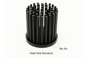
Some people have proposed cylindrical fin structure that can be used for packaging high-power LED modules, while others have proposed using closed micro-jet cooling system to achieve high-power and high-density packaging of LED chips, but the system is much more complex in this way. To reduce thermal impedance, many foreign LED manufacturers place LED chips on the surface of heat sinks made of copper and ceramic materials, and then weld printed circuit boards with wires to heat sinks forced to cool by cooling fans. Panasonic electric has developed a PCB and packaging integration technology, the company will 1mm square blue LED in flip chip packaging on the ceramic substrate, and then paste the ceramic substrate on the copper PCB table
Panasonic says the thermal impedance of the entire module, including the printed circuit board, is about 15K•w-1.Toshiba Lighting has used more than 60lm•w-1 white LED since 2006 to improve thermal conductivity by using lamps and frames, or to design the heat dissipation of Lighting equipment by forced air cooling with cooling fan. The module structure without special heat dissipation technology can also use white LED.
2.5 packaging materials
About the service life of the LED, for example, to switch to the siliceous materials and ceramic packaging materials, can improve the service life of leds, especially the white LED the luminous wavelength spectrum contains less than 450 nm wavelength light, traditional epoxy encapsulating materials are easily destroyed by short wavelength light, high power white LED for big quantity of light more accelerated degradation of encapsulation material, so the packaging materials must be resistant to short wavelength and ultraviolet light, but also has a certain hardness to resist the external mechanical forces and heat resistance, insulation, anti-static, wet resistance are also must pay attention to. More importantly, you must export as much light as possible, whether you want it to be bright or not. Because if the light cannot be successfully exported, the light will be absorbed in the packaging layer and will be converted into heat energy, which adds another worry factor to the packaging heat dissipation problem. In fact, if the heat of LED cannot be successfully discharged and reduced, it will become a heat load, which in turn will damage the LED body, including brightness.
The main packaging materials are adhesive materials, phosphor powder, filling and sealing adhesive, heat dissipation substrate, shell and so on. Bonding materials and substrates are the key links of LED heat dissipation, and appropriate bonding materials and substrates need to be selected according to different applications. The key to the improvement of light output rate lies in the selection and application of sealant and phosphor powder. In fact, the heat dissipation capacity of the chip side surface and the upper surface is extremely poor. Therefore, the heat generated by LED is mostly transmitted to the heat sink at the bottom of the chip by heat conduction, and then dissipated by heat convection. The heat dissipation structure of both conventional chip and flip chip has a bond layer, and the thermal conductivity of binder is the smallest among all heat transfer structures, so the bond layer has the most serious influence on the heat dissipation of chip.LED core and coated phosphors are produced in a few hundred degrees of high temperature conditions, itself has a certain temperature resistance, so packaging is not the first consideration.
2.5.1 shell
The progress of the production technology of the light-emitting tube, high-power light-emitting tube internal thermal resistance is more and more low, the luminous tube is 1W the thermal resistance of common below 15℃, W-1, that is to say, the luminous tube, 1W tube core is higher than the temperature of the tube shell only 15℃.According to the luminous tube core materials heat resistance level, tube core temperature does not exceed 150 ℃ can work for a long time. As a result, the shell temperature of 135℃ is safe to use. But, because of the limitation of shell packaging materials in the actual use shell temperature had better not exceed 70℃, such tube core temperature is 85℃, luminous tube transparent
Packaging materials will not rapidly aging. There is no problem with long-term stable operation, so it is not necessary to reduce the temperature of the semiconductor lamp operating very low, but it is necessary to reduce the thermal resistance between the light-emitting tube shell and the lamp body shell. There is a thermal resistance between the shell and the core of LED, which makes the temperature difference between the shell and the core appear in the use of LED. The temperature of the core will be higher than that of the shell. Therefore, shell design and packaging are also the key technologies. The production of the shell can be based on the requirements of focusing light, the reflective cup can be processed into a cone or parabola shape, the role of the reflective cup is to collect the photons emitted from the chip around the maximum efficiency, the surface finish of the reflective cup has a great relationship with the reflectivity. In the heat structure design of the lamp body, the heat generated by the luminous tube should be successfully transmitted to the shell, and the contact surface between the shell and air should be increased to facilitate the flow of air on the surface of the shell.
2.5.2 substrate
Due to the high-density integration of light-emitting chips, the temperature on the cooling substrate is very high. Therefore, the substrate material with high thermal conductivity and appropriate packaging technology must be adopted to reduce the packaging thermal resistance. For LED packaging devices, thermal resistance mainly includes internal thermal resistance and interface thermal resistance of materials (heat dissipation substrate and heat sink structure).The role of the heat dissipation substrate is to absorb the heat generated by the chip and conduct it to the heat sink to realize heat exchange with the outside world. Common heat dissipation substrate materials include silicon, metals (such as aluminum, copper), ceramics (such as Al2O3, AlN, SiC) and composite materials. Among them, silicon and ceramic material processing difficulties, high cost; The thermal expansion coefficient and ratio of metallic materials are very large, which are difficult to meet the requirements of high-density packaging. Metal matrix composites (such as AlSiC) can combine the high thermal conductivity of metal material (Al) with the low thermal expansion coefficient of reinforced material (SiC), which has the advantages of high thermal conductivity, adjustable thermal expansion coefficient, small specific gravity, high strength and hardness, and has been applied in high-power LED packaging. Al-sic composite substrate shows excellent performance and can be used as an excellent new high-power LED packaging substrate material.
2.5.3 bonding materials
The choice of different chip bonding materials has a great impact on its thermal resistance. The adoption of high-power chip bonding materials can significantly improve the heat dissipation characteristics of high-power LED and effectively reduce the PN junction temperature of the device, so as to maintain the luminosity and chromaticity performance of the power LED device and improve the life of the device. However, power leds that use ordinary heat sink adhesive as chip bonding material have a higher thermal resistance and higher PN junction temperature, so they cannot be used as chip bonding material of power leds. When the input power of power LED devices is further increased to more than 3 W, conductive chip adhesives and other materials with good thermal conductivity cannot meet the requirements of heat dissipation performance of devices. Reducing the printing or coating thickness of the bonding material of the chip can reduce its thermal resistance, but it is difficult to guarantee the mechanical strength between the chip and the pipe base when the thickness is too low, which will affect the damage of the device in the process of reflow welding or other welding methods. The thickness of the bonding material of the chip can neither be too thick nor too thin.
3 conclusion
With the successful development of high-power LED chips above the w-level, their application potential in the field of lighting has been greatly improved. However, the improvement of input power means that more heat needs to be effectively emitted from the PN junction area of the chip. Therefore, high-current working power LED chip, low thermal resistance, good heat dissipation package structure has become the key technology. When designing LED light emitting devices, good heat dissipation design is mainly due to the following considerations: on the one hand, improve the internal packaging structure of devices, find suitable materials, and improve the heat transfer ability of heating chips to the shell; On the other hand, improve the shell to the outside of the ability to heat.